

Semiconductors reach the quantum world
Quantum effects in superconductors could give semiconductor technology a new twist. Researchers at the Paul Scherrer Institute PSI and Cornell University in New York State have identified a composite material that could integrate quantum devices into semiconductor technology, making electronic components significantly more powerful.


Our current electronic infrastructure is based primarily on semiconductors. This class of materials emerged around the middle of the 20th century and has been improved ever since. Among the most important challenges currently facing semiconductor electronics are further improvements that would increase the bandwidth of data transmission, energy efficiency and information security. Incorporating quantum effects is likely to bring about a breakthrough in this regard.
Quantum effects, which can occur in superconducting materials, are particularly conceivable here. Superconductors are materials in which the electrical resistance disappears as soon as they are cooled to a certain temperature. The fact that quantum effects can also be exploited in superconductors has already been demonstrated in the first quantum computers.
In order to find possible successors for today's semiconductor electronics, some researchers - including a group at Cornell University - are investigating so-called heterostructures, i.e. structures made of two different types of materials. More specifically, they are interested in layered systems of superconducting and semiconducting materials. "It has been known for a long time that you have to choose materials with very similar crystal structures so that there is no tension in the crystal lattice at the contact surface," explains John Wright, who produced the heterostructures for the new study at Cornell University.
Two suitable materials in this respect are the superconductor niobium nitride (NbN) and the semiconductor gallium nitride (GaN). The latter already plays an important role in semiconductor electronics and is therefore already well researched. Until now, however, it was unclear how exactly the electrons behave at the contact surface of these two materials - and whether it is possible that the electrons from the semiconductor interfere with the superconductivity and thus cancel out the quantum effects.
"When I came across the research of the group at Cornell, I knew: Here at PSI we can find the answer to this fundamental question with our spectroscopic methods at the ADRESS beamline," explains Vladimir Strocov, a researcher at the Swiss Synchrotron Light Source SLS at PSI.
This is how the two groups came to work together. In their experiments, they finally found that the electrons in both materials keep to themselves. No unwanted interactions take place that could hinder the quantum effects.
Synchrotron light reveals the electronic structures
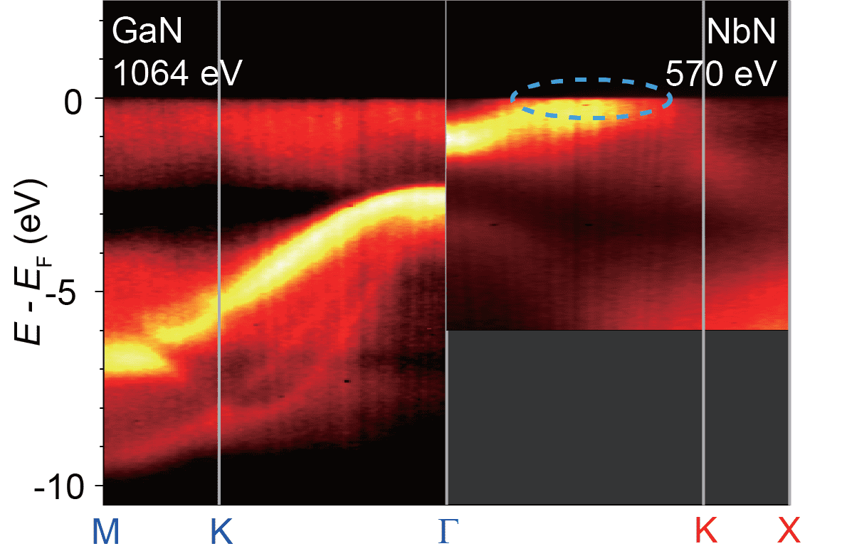
The PSI researchers used a method established at the ADRESS beamline of the SLS: Angle-resolved photoelectron spectroscopy using soft X-rays - abbreviated SX-ARPES in English. "This method allows us to visualize the collective motion of electrons in the material," explains Tianlun Yu, a postdoctoral researcher on Vladimir Strocov's team who performed the measurements on the NbN/GaN heterostructure. Together with Wright, Yu is first author of the new publication.
The SX-ARPES method provides a kind of map whose spatial coordinates show the energy of the electrons in one direction and something like their velocity in the other; more precisely, their momentum. "In this representation, the electronic states show up as bright bands in the map," Yu explains. The crucial research result: at the material boundary between the niobium nitride NbN and the gallium nitride GaN, the respective "bands" are clearly separated from each other. From this, the researchers were able to read: The electrons remain in their original material and do not interact with the electrons in the neighbouring material.
"The most important conclusion for us is that superconductivity in niobium nitride remains undisturbed even when this is suitably deposited atom by atom on a layer of gallium nitride," says Vladimir Strocov. "This allowed us to provide another piece of the puzzle that confirms: This layer system could indeed give rise to a new form of semiconductor electronics that embeds and exploits the quantum effects in superconductors."
Original publication: Momentum-resolved electronic structure and band offsets in an epitaxial NbN/GaN superconductor/semiconductor heterojunction; T. Yu, J. Wright, G. Khalsa, B. Pamuk, C. S. Chang, Y. Matveyev, X. Wang, T. Schmitt, D. Feng, D. A. Muller, H. G. Xing, D. Jena, V. N. Strocov; Science Advances, 22 December 2021 (online) DOI: 10.1126/sciadv.abi5833